Products
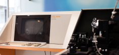
Optical Instruments(Santec LIS Corporation)
Optical Imaging / Sensing(Santec LIS Corporation)
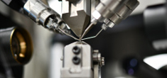
Optical Components(Santec AOC Corporation)
Medical Devices(Santec OIS Corporation)
MOGLabs Products(Santec LIS Corporation)
About Us
CEO Greeting
Management Team
Santec Policy
History
Key Facts
Group Companies
Core Technology
Quality & Environmental Policy
Investors
Investors (Japanese)
Markets & Applications
Financial Highlights
IR Library (Japanese)
IR Policy
IR Calendar
Financial Statements
FAQs
Public Notice (Japanese)
Support
Operation Manual
Data Sheets
Software Downloads
Transportation Precautions
Discontinued Products and Support